What are the common production processes for digital integrated circuits?
Common Production Processes for Digital Integrated Circuits
I. Introduction
Digital integrated circuits (ICs) are the backbone of modern electronic devices, enabling everything from smartphones to supercomputers. These circuits consist of numerous interconnected components, such as transistors, resistors, and capacitors, all integrated onto a single semiconductor chip. The importance of digital ICs cannot be overstated; they are essential for processing and storing data, controlling devices, and facilitating communication in our increasingly digital world. This blog post will explore the common production processes involved in creating digital integrated circuits, from the initial design phase to final testing and quality assurance.
II. Design Phase
The production of digital ICs begins with a comprehensive design phase, which is crucial for ensuring that the final product meets the required specifications and performance standards.
A. Conceptualization and Specification
The first step in the design phase involves gathering requirements and defining functional specifications. Engineers and designers collaborate to understand the intended application of the IC, which informs decisions about its architecture, performance, and power consumption. This stage is critical, as any misalignment between the specifications and the final product can lead to costly redesigns.
B. Schematic Design
Once the specifications are established, the next step is schematic design. Designers use specialized circuit design tools to create a visual representation of the circuit, detailing how each component will interact. Simulation and verification are integral to this process, allowing designers to test the circuit's functionality and performance under various conditions before moving on to the physical layout.
C. Layout Design
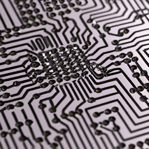
The layout design phase involves translating the schematic into a physical representation that can be fabricated. Designers utilize physical design tools to arrange the components on the chip, ensuring that they fit within the specified dimensions and adhere to design rules. Design Rule Checking (DRC) is performed to verify that the layout complies with manufacturing constraints, such as minimum spacing between components and layer thickness.
III. Fabrication Process
After the design phase is complete, the fabrication process begins. This stage involves several intricate steps to create the physical IC from the designed layout.
A. Wafer Preparation
The fabrication process starts with wafer preparation. Silicon wafers, typically 200mm or 300mm in diameter, are produced from high-purity silicon crystals. The wafers undergo a thorough cleaning process to remove any contaminants that could affect the subsequent steps.
B. Photolithography
Photolithography is a critical step in the fabrication process. A photoresist material is applied to the wafer's surface, which is then exposed to ultraviolet (UV) light through a mask that contains the circuit pattern. The exposed areas of the photoresist undergo a chemical change, allowing for selective development. This process creates a patterned layer that will guide the etching and doping processes.
C. Etching
Etching is used to remove unwanted material from the wafer, transferring the pattern created during photolithography. There are two main types of etching: wet etching, which uses chemical solutions, and dry etching, which employs plasma. The choice of etching method depends on the specific requirements of the circuit design and the materials involved.
D. Ion Implantation
Ion implantation is a technique used to introduce impurities, or dopants, into the silicon wafer to modify its electrical properties. This process allows for the precise control of the semiconductor's conductivity, enabling the creation of p-type and n-type regions essential for transistor operation.
E. Deposition Techniques
Deposition techniques are employed to add thin films of materials onto the wafer. Two common methods are Chemical Vapor Deposition (CVD) and Physical Vapor Deposition (PVD). CVD involves chemical reactions that deposit materials onto the wafer, while PVD uses physical processes, such as sputtering, to create thin films. These layers are crucial for forming interconnections and insulating regions within the IC.
F. Chemical Mechanical Planarization (CMP)
Chemical Mechanical Planarization (CMP) is a process used to achieve a smooth and even surface on the wafer. This step is essential for ensuring layer uniformity and preparing the wafer for subsequent processing steps. CMP combines chemical and mechanical forces to remove excess material and create a flat surface.
IV. Assembly and Packaging
Once the fabrication process is complete, the next phase is assembly and packaging, which prepares the IC for integration into electronic devices.
A. Die Preparation
The first step in assembly is die preparation, where the wafer is diced into individual chips, or dies. Each die contains a complete circuit that will be packaged for use. After dicing, the dies are attached to a substrate or package using die attach materials.
B. Wire Bonding and Flip-Chip Bonding
To establish electrical connections between the die and the package, wire bonding or flip-chip bonding techniques are employed. Wire bonding involves using fine wires to connect the die's pads to the package leads, while flip-chip technology flips the die upside down and connects it directly to the package using solder bumps. Each method has its advantages, depending on the application and performance requirements.
C. Packaging Types
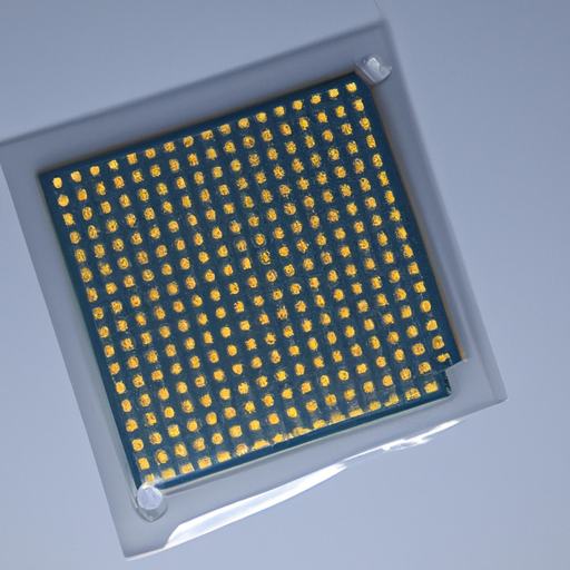
The choice of packaging type is crucial for protecting the IC and ensuring reliable performance. Common packaging types include Dual In-line Package (DIP), Surface Mount Device (SMD), and Ball Grid Array (BGA). Each type offers different benefits in terms of size, thermal performance, and ease of assembly.
V. Testing and Quality Assurance
After assembly, the ICs undergo rigorous testing and quality assurance to ensure they meet performance standards and reliability requirements.
A. Functional Testing
Functional testing is the first step in quality assurance, where the ICs are subjected to various test patterns using specialized equipment. Automated Test Equipment (ATE) is commonly used to perform these tests, allowing for efficient and accurate evaluation of the IC's functionality.
B. Reliability Testing
Reliability testing assesses the IC's performance under extreme conditions. Stress testing simulates high temperatures, voltages, and other environmental factors to identify potential failure modes. Environmental testing evaluates the IC's performance in different humidity and temperature conditions, ensuring it can withstand real-world usage.
C. Yield Analysis
Yield analysis is a critical aspect of the production process, focusing on measuring defect density and overall yield rates. By identifying and addressing defects, manufacturers can implement yield improvement strategies, ultimately enhancing the efficiency and profitability of the production process.
VI. Conclusion
The production of digital integrated circuits involves a complex interplay of design, fabrication, assembly, and testing processes. Each stage is crucial for ensuring that the final product meets the required specifications and performance standards. As technology continues to advance, the production processes for digital ICs are evolving, with trends such as miniaturization, increased integration, and the adoption of new materials shaping the future of semiconductor manufacturing. Innovation will play a vital role in driving these changes, enabling the development of more powerful and efficient digital integrated circuits that will continue to power our modern world.
VII. References
- Academic Journals
- Industry Reports
- Textbooks on Semiconductor Manufacturing
This blog post provides a comprehensive overview of the common production processes for digital integrated circuits, highlighting the intricate steps involved in bringing these essential components to life. Each section can be further expanded with specific examples, case studies, or recent advancements in technology to enhance the depth of the discussion.


